Premium content
Access to this content requires a subscription. You must be a premium user to view this content.

Would you like to see your presentation here, made available to a global audience of researchers?
Add your own presentation or have us affordably record your next conference.
Electrically driven magnetization switch utilizing voltage-controlled magnetic anisotropy (VCMA) have attracted much attention in the new generation memory, especially
for spin-orbit torque (SOT)-based magnetic random access memory (MRAM) 1,2. For the traditional SOT switching, an additional magnetic field is needed to break the inversion
symmetry, which makes the circuit difficult to implement 3. Combining the SOT with the VCMA effect can realize the certain switching in SOT-MRAM with lower critical switching
current 4. With the development of the SOT-MRAM, device model is urgently needed for the device characterization. However, the published models are facing limitations as the size shrinks down
to nanometer. Also, the effect of the elevated temperature caused by repeated operation on the device is non-negligible 5. Therefore, an effective model is needed to represent the
switching dynamic of the device concerning the influence of the nanoscale and the thermal effect.
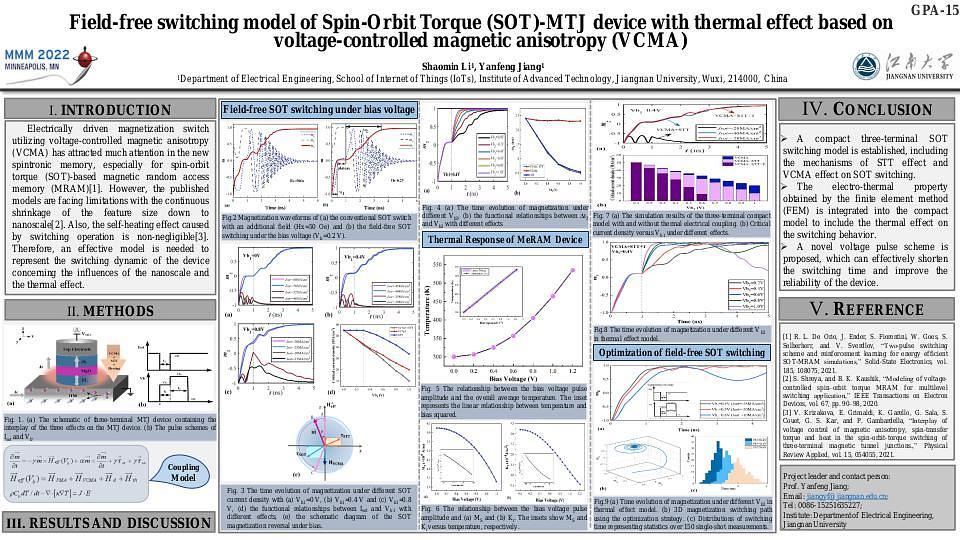
In the paper, a compact model of three-terminal VCMA assisted SOT switching is established. The influence of the VCMA effect on the field-free SOT switching is considered by
numerically solving the LLG equations. Furthermore, a 3D model of the VCMA+SOT device is established by finite element method to demonstrate the thermoelectric behavior.
Considering the influence of the thermal effect generated in the working state on the switching characteristics, the electrothermal behavior is integrated into the compact model to show the
influence of the temperature on the switching behavior, highlighting the importance of the thermal effect for the realistic modelling of SOT switching. Additionally, considering the
influence of thermal effect, the switching error rate of the device under different working voltage conditions is evaluated. Finally, a novel voltage pulse scheme is proposed, which can
effectively shorten the inversion time and improve the reliability of the device. The established model provides strategies and guidelines for next-generation memory design and
application.
References
1 W. Kang, Y. Ran and Y. G. Zhang et al., IEEE Trans. Nanotechnol., Vol. 16, p. 387 (2017).
2 S. Sharmin, A. Jaiswal, and K. Roy, IEEE Trans. Electron Devices, vol. 63, p. 3493 (2016).
3 A. Manchon, I. M. Miron and T. Jungwirth et al., Rev. Mod. Phys., vol. 91, p. 035004 (2019).
4 S. Shreya and B. K. Kaushik, IEEE Trans. Electron Devices, vol. 67, p. 90 (2019).
5 J. J. Kan, C. Park and C. Ching et al., IEEE Trans. Electron Devices, vol. 64, p. 3639 (2017).

Fig.1 Schematics of the three-terminal device allowing for field-free SOT switching with an illustration of the influences of VCMA and thermal effects.

